The analog voltage source must be able to
charge the sample and hold (S/H) capacitor in the ADC in order to achieve maximum accuracy.
Seen externally the ADC input consists of a resistor (RSAMPLE) and a capacitor (CSAMPLE). In addition, the source resistance (RSOURCE) must be taken into account when calculating the required
sample and hold time. The next figure shows the ADC input channel equivalent circuit.
Figure 1. ADC Input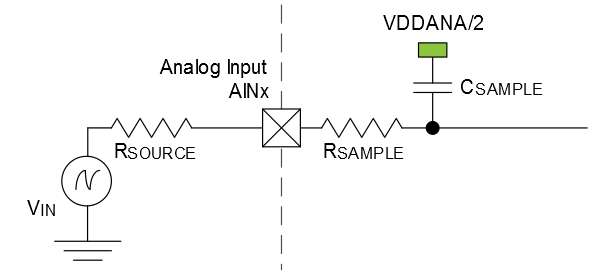
To achieve n bits of accuracy, the CSAMPLE capacitor must be charged at least to a voltage of
VCSAMPLE≥VIN×1+−2−n+1
The minimum sampling time tSAMPLEHOLD for a given RSOURCEcan be found using this formula:
tSAMPLEHOLD≥RSAMPLE+RSOURCE×CSAMPLE×n+1×ln2
for a 12 bits accuracy: tSAMPLEHOLD≥RSAMPLE+RSOURCE×CSAMPLE×9.02
where
tSAMPLEHOLD=12×fADC