To avoid data collisions, the SPI peripheral can be configured in buffered mode
by writing a '1' to the Buffer Mode Enable bit (CTRLB.BUFEN) in the Control B register
(SPI.CTRLB). In this mode, the SPI has additional interrupt flags and extra buffers. The
extra buffers are shown in Figure 1. There are two different modes for the buffer mode,
selected with the Buffer Mode Wait for Receive bit (BUFWR). The two different modes are
described below with timing diagrams.
Figure 1. SPI Timing Diagram in buffer mode
with CTRLB.BUFWR set to zero
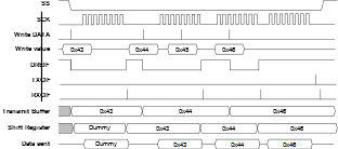
All writes to the Data Register (DATA) goes to the Transmit Buffer Register. As the
figure above shows 0x43 is written to the Data Register (DATA), but it is not immediately
transferred to the shift register so the first byte sent will be a dummy byte. The value of
the dummy byte is whatever was in the shift register at the time, usually the last received
byte. After the first dummy transfer is completed the value 0x43 is transferred to the
shift register. Then 0x44 is written to the Data Register (DATA) and goes to the Transmit
Buffer Register. A new transfer is started and 0x43 will be sent. The value 0x45 is written
to the Data Register (DATA), but the Transmit Buffer Register is not updated since it is
already full containing 0x44 and the Data Register Empty Interrupt Flag (INTFLAGS.DREIF) is
low. The value 0x45 will be lost. After the transfer the value 0x44 is moved to the shift
register. During the next transfer 0x46 is written to the Data Register (DATA) and 0x44 is
sent out. After the transfer is complete 0x46 is copied into the shift register and it is
sent out in the next transfer.
The Data Register Empty Interrupt Flag (INTFLAGS.DREIF) goes low every time
the Transmit Buffer Register is written and goes high after a transfer when the previous
value in the Transmit Buffer Register is copied into the shift register. The Receive
Complete Interrupt Flag (INTFLAGS.RXCIF) is set one cycle after the Data Register Empty
Interrupt Flag (INTFLAGS.DREIF) goes high. The Transfer Complete Interrupt Flag
(INTFLAGS.TXCIF) is set one cycle after the Receive Complete Interrupt Flag
(INTFLAGS.RXCIF) is set when both the value in the shift register and the Transmit Buffer
Register has been sent.
Figure 2. SPI Timing Diagram in buffer mode
with CTRLB.BUFWR set to one
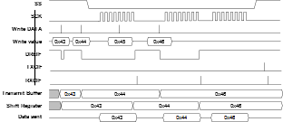
All writes to the Data Register (DATA) goes to the transmit buffer. As the figure
above shows 0x43 is written to the Data Register (DATA) and since the Slave Select pin is
high it is copied to the shift register the next cycle. Then the next write (0x44) will go
to the Transmit Buffer Register. During the first transfer the value 0x43 will be shifted
out. In the figure the value 0x45 is written to the Data Register (DATA), but the Transmit
Buffer Register is not updated since the Data Register Empty Interrupt Flag
(INTFLAGS.DREIF) is low. After the transfer is completed the value 0x44 form the Transmit
Buffer Register is copied over to the shift register. The value 0x46 is written to the
Transmit Buffer Register. During the next two transfers 0x44 and 0x46 is shifted out. The
Flags behaves the same as with Buffer Mode Wait for Receive Bit (CTRLB.BUFWR) set to zero.