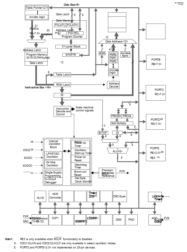
Devices in the PIC18F26/45/46Q10 family are available in 28-pin and 40/44-pin packages. The block diagram for this device is shown in Figure 1.
The devices have the following differences:
- 1.Program Flash Memory
- 2.Data Memory SRAM
- 3.Data Memory EEPROM
- 4.A/D channels
- 5.I/O ports
- 6.Enhanced USART
- 7.Input Voltage Range/Power Consumption
All other features for devices in this family are identical. These are summarized in the following Device Features table.
The pinouts for all devices are listed in the pin summary tables.
| Features | PIC18F26Q10 | PIC18F45Q10 | PIC18F46Q10 |
|---|---|---|---|
| Program Memory (Bytes) |
65536 |
32768 |
65536 |
| Program Memory (Instructions) |
32768 |
16384 |
32768 |
| Data Memory (Bytes) |
3615 |
2048 |
3615 |
| Data EEPROM Memory (Bytes) |
1024 |
256 |
1024 |
| I/O Ports | A,B,C,E(1) |
A,B,C,D,E |
A,B,C,D,E |
| Capture/Compare/PWM Modules (CCP) | 2 | 2 | 2 |
| 10-Bit Pulse-Width Modulator (PWM) | 2 | 2 | 2 |
| 10-Bit Analog-to-Digital Module (ADC2) with Computation Accelerator | 4 internal 24 external |
4 internal 35 external |
4 internal 35 external |
| Packages |
28-pin SPDIP |
40-pin PDIP |
40-pin PDIP |
| Timers (16-/8-bit) | 4/3 | 4/3 | 4/3 |
| Serial Communications | 2 MSSP, 2 EUSART |
2 MSSP, 2 EUSART |
2 MSSP, 2 EUSART |
| Enhanced Complementary Waveform Generator (ECWG) | 1 | 1 | 1 |
| Zero-Cross Detect (ZCD) | 1 | 1 | 1 |
| Data Signal Modulator (DSM) | 1 | 1 | 1 |
| Configurable Logic Cell (CLC) | 8 | 8 | 8 |
| Peripheral Pin Select (PPS) | Yes | Yes | Yes |
| Peripheral Module Disable (PMD) | Yes | Yes | Yes |
| 16-bit CRC with NVMSCAN | Yes | Yes | Yes |
| Programmable High/Low-Voltage Detect (HLVD) | Yes | Yes | Yes |
| Programmable Brown-out Reset (BOR) | Yes | Yes | Yes |
| Resets (and Delays) | POR, BOR, RESET Instruction, Stack Overflow, Stack Underflow (PWRT, OST), MCLR, WDT |
POR, BOR, RESET Instruction, Stack Overflow, Stack Underflow (PWRT, OST), MCLR, WDT |
POR, BOR, RESET Instruction, Stack Overflow, Stack Underflow (PWRT, OST), MCLR, WDT |
| Instruction Set | 75 Instructions; 83 with Extended Instruction Set enabled |
75 Instructions; 83 with Extended Instruction Set enabled |
75 Instructions; 83 with Extended Instruction Set enabled |
| Operating Frequency | DC – 64 MHz | DC – 64 MHz | DC – 64 MHz |
| Note 1: PORTE contains the single RE3 read-only bit. | |||