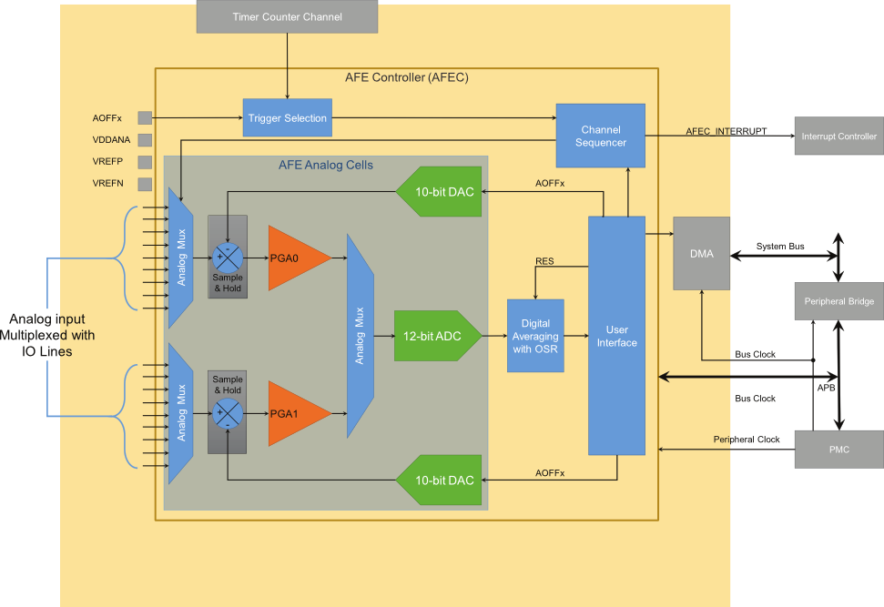
The Analog Front-End Controller (AFEC) is based on an Analog Front-End cell (AFE) integrating a 12-bit Analog-to-Digital Converter (ADC), a Programmable Gain Amplifier (PGA), a Digital-to-Analog Converter (DAC) and a 12-to-1 analog multiplexer, making possible the analog-to-digital conversions of 12 analog lines. two 6-to-1 analog multiplexers, making possible the analog-to-digital conversions of 12 analog lines (in single Sample-and-Hold mode) or two simultaneous conversions of 6 analog lines (in dual Sample-and-Hold mode). The conversions extend from 0V to ADVREFP. The AFEC supports an 10-bit or 12-bit resolution mode which can be extended up to a 16-bit resolution by digital averaging.
Conversion results are reported in a common register for all channels, as well as in a channel-dedicated register.
Software trigger, external trigger on rising edge of the AFE_ADTRG pin or internal triggers from Timer Counter output(s) are configurable.
The comparison circuitry allows automatic detection of values below a threshold, higher than a threshold, in a given range or outside the range. Thresholds and ranges are fully configurable.
The AFEC internal fault output is directly connected to PWM Fault input. This input can be asserted by means of comparison circuitry in order to immediately put the PWM outputs in a safe state (pure combinational path).
The AFEC also integrates a Sleep mode and a conversion sequencer and connects with a DMA channel. These features reduce both power consumption and processor intervention.
The AFEC has a selectable single-ended or fully differential input and benefits from a 2-bit programmable gain. A set of reference voltages is generated internally from a single external reference voltage node that may be equal to the analog supply voltage.
The AFEC is powered by the analog power domain (VDDANA) and VREFP is the positive reference of the AFE. The VREFN pin must be connected to ground.
DAC1 and DAC0 provide an analog output voltage (VDAC) in the range [0 : VREFP] with an accuracy equal to 10 bits. The DAC output voltage is single-ended and is used as a reference node by the sampling stage S/H0 and S/H1 (Sample-and-Hold PGA), relative to the single-ended input signal being sampled on the selected channel.
As a consequence, programming the DAC output voltage offers a capability to compensate for a DC offset on the input signal being sampled. DC offset compensation is effective in single-ended operation and is not effective in fully differential operation.