After the conversion is complete (ADCSRA.ADIF is set), the conversion result can be found in the ADC Result Registers (ADCL, ADCH).
For single ended conversion, the result is
where VIN is the voltage on the selected input pin, and VREF the selected voltage reference (see also descriptions of ADMUX.REFSn and ADMUX.MUX). 0x000 represents analog ground, and 0x3FF represents the selected reference voltage minus one LSB.
If differential channels are used, the result is
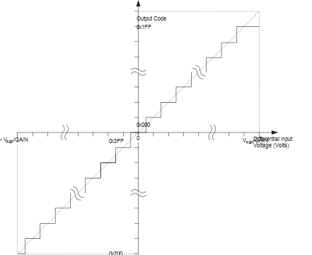
where VPOS is the voltage on the positive input pin, VNEG the voltage on the negative input pin, GAIN the selected gain factor, and VREF the selected voltage reference. The result is presented in two’s complement form, from 0x200 (-512d) through 0x1FF (+511d). Note that if the user wants to perform a quick polarity check of the results, it is sufficient to read the MSB of the result (ADC9 in ADCH). If this bit is one, the result is negative, and if this bit is zero, the result is positive. The figure below shows the decoding of the differential input range.
| VADCn | Read code | Corresponding Decimal Value |
|---|---|---|
| VADCm + VREF/GAIN | 0x1FF | 511 |
| VADCm + 0.999 VREF/GAIN | 0x1FF | 511 |
| VADCm + 0.998 VREF/GAIN | 0x1FE | 510 |
| ... | ... | ... |
| VADCm + 0.001 VREF/GAIN | 0x001 | 1 |
| VADCm | 0x000 | 0 |
| VADCm - 0.001 VREF/GAIN | 0x3FF | -1 |
| ... | ... | ... |
| VADCm - 0.999 VREF/GAIN | 0x201 | -511 |
| VADCm - VREF/GAIN | 0x200 | -512 |
Example:
ADMUX = 0xED (ADC3 - ADC2, 10× gain, 2.56V reference, left adjusted result)
Voltage on ADC3 is 300 mV, voltage on ADC2 is 500 mV.
ADCR = 512 × 10 × (300 - 500) / 2560 = -400 = 0x270
ADCL will thus read 0x00, and ADCH will read 0x9C.
Writing zero to ADLAR right adjusts the result: ADCL = 0x70, ADCH = 0x02.