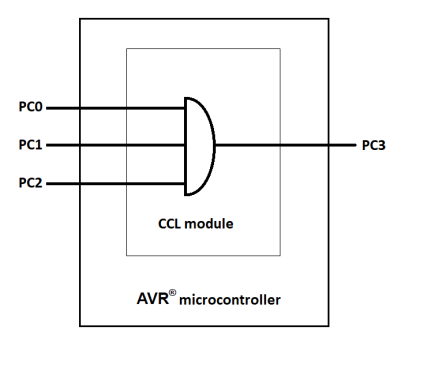
The CCL module can be used to implement a logic gate with up to three inputs. The following example shows how to configure and use CCL LUT1 to implement an AND gate.


The table below summarizes the INSEL[3:0] options for all inputs.
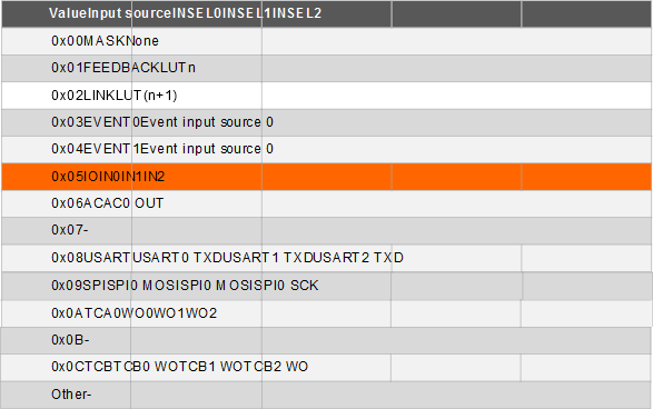
This translates to the following code:
CCL.LUT1CTRLB = CCL_INSEL0_IO_gc | CCL_INSEL1_IO_gc;

CCL.LUT1CTRLC = CCL_INSEL2_IO_gc;
The next step is to configure the Truth tables for LUT1 to generate the right combinational logic to implement an AND gate on the selected pins. Thus, the Truth table will have a value of 0x80.
CCL.TRUTH1 = 0x80;The next step is to configure the output of decoder, specifically, the I/O Port pin (PC3) in this example. This is done by setting the OUTEN bit on the LUT0CTRLA register.

This translates to the following code:
CCL.LUT1CTRLA = CCL_OUTEN_bm;By enabling the LUTn output on the I/O pin, the settings for the corresponding pin are overwritten. To enable the decoding of the input sequence, the CCL and the used LUTs need to be enabled. That is done using the ENABLE bit from the LUTnCTRLA register.
CCL.LUT1CTRLA |= CCL_ENABLE_bm;To complete the setup, the CCL module should also be enabled using a CCL global Enable bit from the CTRLA register.

CCL.CTRLA = CCL_ENABLE_bm;