Use case description: TCB (the TCB3 instance) will be configured in 8-bit PWM mode and generate a 1-second period PWM signal, at a 50% duty cycle. A GPIO pin (Port B pin 5 - PB5) will be used as an output to showcase the signal.
Result: TCB will generate a 50% duty cycle PWM signal for a 1-second period. The on-board LED (the PB5 pin) will toggle every 500 ms.
This timer can be configured to run in 8-bit PWM mode where each of the register pairs in the 16-bit Capture/Compare register (TCBn.CCMPH and TCBn.CCMPL) is used as an individual compare register. The counter will continuously count from zero to CCMPL and the output will be set at BOTTOM and cleared when the counter reaches CCMPH.
- 1.Disable the peripheral.
- 2.Write Capture/Compare register to {CCMPH, CCMPL}.
- 3.Write 0x0000 to count register.
- 4.Re-enable the module.
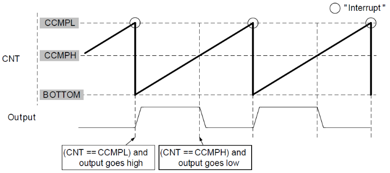
For example, for a 256 Hz frequency clock that serves as input to the timer, the result is a 1-second period (CCMPL is an 8-bit register, which means it can have values from 0 to 255).
Configuring a pin as output for visualizing the PWM signal
To visualize the PWM, a pin will be configured in the Output mode. The following code sets PB5 as output low.
PORTB_DIR |= PIN5_bm;
PORTB_OUT |= PIN5_bm;
Configuring the system clock
According to the diagram in Figure 1, there are two main clock sources for TCB:
- CLK_PER (the peripheral clock, derived from main clock CLK_MAIN)
- CLK_TCA (the TCA clock, which can be derived from CLK_PER)
For the purpose of this use case of TCB, CLK_PER clock source and instance 3 of TCB will be used (TCB3). In order to get a 1-second period, the input clock must be as low as possible. The following configuration must be made:
- Internal 32 kHz ultra low-power oscillator for CLKSEL must be selected
- The clock prescaler (PEN) must be enabled
- The highest prescaler division (PDIV 64) must be used
In order to use the 32 kHz internal oscillator as clock source for TCB, the user must configure the following registers and bits or bit fields in the following register.
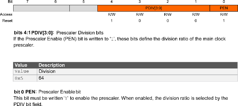
The Main Clock and Prescaler Configuration registers (CLKCTRL.MCLKCTRLA, CLKCTRL.MCLKCTRLB) are protected by the Configuration Change Protection (CCP) mechanism, employing a timed-write procedure for changing these registers. In order to write to these registers, a certain key must be written to the CPU.CCP register first, followed by a write access to the protected bits within four CPU instructions.
READ/WRITE instruction and the change must be
made in the following four cycles, after writing the key.CPU_CCP = CCP_IOREG_gc;Since the desired frequency is the lowest possible, the Prescaler (PEN) must be enabled and PDIV must be set to ‘64’ divider.
CLKCTRL.MCLKCTRLB = CLKCTRL_PDIV_64X_gc | CLKCTRL_PEN_bm;
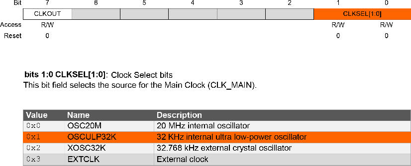
OSCULP32K must be selected, which means CLKSEL bit field must be set to 0x1 value. This translates into the following code:
CLKCTRL.MCLKCTRLA = CLKCTRL_CLKSEL_OSCULP32K_gc;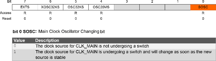
The clock switching process is indicated by the SOSC bit. The program should halt during an undergoing switch of the clock source, so a wait until the switch is over should be implemented:
while (CLKCTRL.MCLKSTATUS & CLKCTRL_SOSC_bm)
{
    ;
}
Configuring the TCB input clock and operation mode
In order to generate the 8-bit PWM signal to PB5, the following registers must be changed:
- TCBn.CCMP
- TCBn.CTRLA
- TCBn.CTRLB
The TCBn.CCMPL and TCBn.CCMPH register pair represents the 16-bit value TCBn.CCMP. The low byte <7:0> (suffix L) is accessible at the original offset. The high byte <15:8> (suffix H) can be accessed at offset +0x01. In 8-bit PWM mode, TCBn.CCMPL and TCBn.CCMPH act as two independent registers.
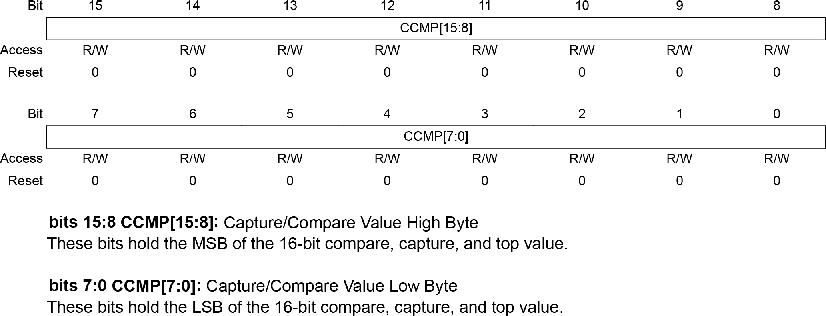
When running TCB in 8-bit PWM mode, TCBn.CCMPL must be loaded with the PWM signal period, of 1 second in this case. Since the period of the output pulse is defined by TCBn.CCMPL+1, the value that must be loaded into the TCBn.CCMPL register is 0xFF (255 in decimal).
Subsequently, TCBn.CCMPH must be loaded with the number of cycles for which the output will be driven high. The goal is to set the duty cycle at 50% in order to make PB5 toggle every 500 ms.
This means that TCBn.CCMP must be loaded with the following value, obtained from TCBn.CCMPH and TCBn.CCMPL:
TCB3.CCMP = 0x80FF;
TCB3 can be enabled by setting the ENABLE bit to ‘1’ in the
TCB3.CTRLA register. This translates into the following code:
TCB3.CTRLA |= TCB_ENABLE_bm;In order to get the lowest possible frequency, CLK_PER will be further divided by 2, by configuring the CLKSEL bit field in the TCB3.CTRLA register. The corresponding value for CLKSEL in this case is 0x1. This translates into the following code:
TCB3.CTRLA |= TCB_CLKSEL_CLKDIV2_gc;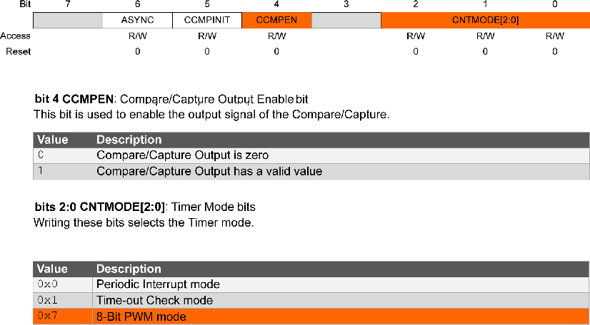
CCMPEN must be enabled. This translates into the following code:
TCB3.CTRLB |= TCB_CCMPEN_bm;TCB must be configured for the 8-bit PWM mode. This translates to the following code:
TCB3.CTRLB |= TCB_CNTMODE_PWM8_gc;