- Slice 0 DTI0 / SWAP0 acting on port pins (WO[0], WO[WO_NUM/2 +0])
- Slice 1 DTI1 / SWAP1 acting on port pins (WO[1], WO[WO_NUM/2 +1])
- Slice n DTIx / SWAPx acting on port pins (WO[x], WO[WO_NUM/2 +x])
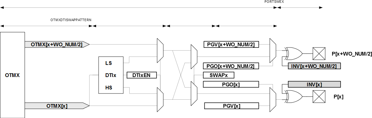
The output matrix (OTMX) unit distributes compare channels, according to the selectable configurations in Table 1.
| Value | OTMX[x] | |||||||
|---|---|---|---|---|---|---|---|---|
| 0x0 | CC3 | CC2 | CC1 | CC0 | CC3 | CC2 | CC1 | CC0 |
| 0x1 | CC1 | CC0 | CC1 | CC0 | CC1 | CC0 | CC1 | CC0 |
| 0x2 | CC0 | CC0 | CC0 | CC0 | CC0 | CC0 | CC0 | CC0 |
| 0x3 | CC1 | CC1 | CC1 | CC1 | CC1 | CC1 | CC1 | CC0 |
Notes on Table 1:
- Configuration 0x0 is the default configuration. The channel location is the default one, and channels are distributed on outputs modulo the number of channels. Channel 0 is routed to the Output matrix output OTMX[0], and Channel 1 to OTMX[1]. If there are more outputs than channels, then channel 0 is duplicated to the Output matrix output OTMX[CC_NUM], channel 1 to OTMX[CC_NUM+1] and so on.
- Configuration 0x1 distributes the
channels on output modulo half the number of channels. This assigns twice the number of
output locations to the lower channels than the default configuration. This can be used,
for example, to control the four transistors of a full bridge using only two compare
channels.
Using pattern generation, some of these four outputs can be overwritten by a constant level, enabling flexible drive of a full bridge in all quadrant configurations.
- Configuration 0x2 distributes compare channel 0 (CC0) to all port pins. With pattern generation, this configuration can control a stepper motor.
- Configuration 0x3 distributes the compare channel CC0 to the first output, and the channel CC1 to all other outputs. Together with pattern generation and the fault extension, this configuration can control up to seven LED strings, with a boost stage.
-
Table 2. Example: four compare channels on four outputs Value OTMX[3] OTMX[2] OTMX[1] OTMX[0] 0x0 CC3 CC2 CC1 CC0 0x1 CC1 CC0 CC1 CC0 0x2 CC0 CC0 CC0 CC0 0x3 CC1 CC1 CC1 CC0
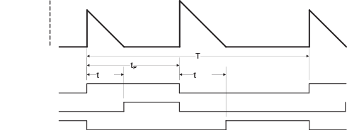
The dead-time insertion (DTI) unit generates OFF time with the non-inverted low side (LS) and inverted high side (HS) of the wave generator output forced at low level. This OFF time is called dead time. Dead-time insertion ensures that the LS and HS will never switch simultaneously.
The DTI stage consists of four equal dead-time insertion generators; one for each of the first four compare channels. Figure 2 shows the block diagram of one DTI generator. The four channels have a common register which controls the dead time, which is independent of high side and low side setting.
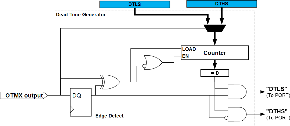
As shown in Figure 3, the 8-bit dead-time counter is decremented by one for each peripheral clock cycle until it reaches zero. A non-zero counter value will force both the low side and high side outputs into their OFF state. When the output matrix (OTMX) output changes, the dead-time counter is reloaded according to the edge of the input. When the output changes from low to high (positive edge) it initiates a counter reload of the DTLS register. When the output changes from high to low (negative edge) it reloads the DTHS register.
The pattern generator unit produces a synchronized bit pattern across the port pins it is connected to. The pattern generation features are primarily intended for handling the commutation sequence in brushless DC motors (BLDC), stepper motors, and full bridge control. See also Figure 4.
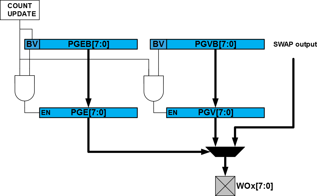
As with other double-buffered timer/counter registers, the register update is synchronized to the UPDATE condition set by the timer/counter waveform generation operation. If synchronization is not required by the application, the software can simply access directly the PATT.PGE, PATT.PGV bits registers.