Inside an ADC, the sample and hold circuit of the ADC contains a resistance-capacitance (RADC and CADC) pair in a low pass filter arrangement. The CADC is also called as sampling capacitor. Whenever an ADC start conversion signal is issued, the sampling switches between the RADC – CADC pair is closed so that the analog input voltage charges the sampling capacitor through the resistance RADC.
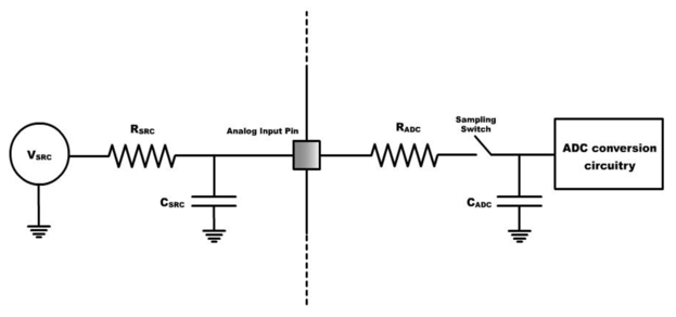
The input impedance of the ADC is the combination of RADC and the impedance of the capacitor. As the sampling capacitor gets charged to the input voltage, the current through RADC reduces and ends up with a minimum value when voltage across the sampling capacitor equals the input voltage. So the minimum input impedance of the ADC equals RADC.
- RADC and CADC are a part of the ADC specification. Refer the device datasheet for more information.
- RSRC and CSRC directly affects the operating speed and accuracy of ADC module. In the practical applications, RSRC and CSRC of the input signal must be considered while selecting the ADC parameters.