The Analog Input Voltage (AIN) is the voltage to be measured and converted into a digital value. The input voltage should always be less than VREF to avoid saturation of the ADC. The input voltage range is also called as conversion range.
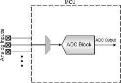
- Single-ended Input
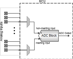
- Differential Input
In differential input, the difference in voltage of two analog inputs is applied to the ADC module. This can be done either directly or after performing some amplification using suitable gain stages. Differential conversions are usually operated in signed mode, where the MSB of the output code acts as the sign bit. When using differential mode, offset error can be measured easily by setting up the positive and negative input on the same pin and the offset can be measured directly as the ADC does not require the Ground (GND) level as a reference.
Most ADCs can operate only using a positive input voltage. The ADCs whose AIN falls in the positive range (0 < AIN < VREF) are called as Unipolar ADC. ADCs capable of accepting both positive and negative input voltages are called as Bipolar ADC(1). For example, in a Unipolar ADC, if the VREF = 2V, then 0 < AIN < 2V should always be maintained to get expected output.
- Refer the respective device datasheet to know the input type, polarity, and input range supported by the device.
- For details about Signed / Unsigned conversion modes of Atmel® AVR® XMEGA® devices, refer to the AVR1300: Using the Atmel AVR XMEGA ADC.