Operating conditions:
- VDD=3V, except where specified otherwise.
| Symbol | Description | Condition | Min. | Typ. | Max. | Unit | |
|---|---|---|---|---|---|---|---|
| fOSC20M | Accuracy with 16MHz Frequency Selection | Factory calibrated | T=25°C, 3.0V | TBD | ±1.5 | TBD | % |
| T=[0, 70]°C, VDD=[1.8, 3.6]V | TBD | ±2 | TBD | ||||
| Full operation range | TBD | ±3 | TBD | ||||
| Accuracy with 20MHz Frequency Selection | Factory calibrated | T=25C, 3.0V | TBD | ±1.5 | TBD | ||
| T=[0, 70]°C, VDD=[1.8, 3.6]V | TBD | ±2 | TBD | ||||
| Full operation range | TBD | ±3 | TBD | ||||
| Accuracy with 16MHz Frequency Selection with factory-stored frequency error value | Factory calibrated VDD=3V(1) | T=[0, 70]°C, VDD=[1.8, 4.5]V | TBD | ±1.5 | TBD | % | |
| Factory calibrated VDD=5V(1) | T=[0, 70]°C, VDD=[4.5, 5.5]V | TBD | ±1.5 | TBD | |||
| Accuracy with 20MHz Frequency Selection with factory-stored frequency error value | Factory calibrated VDD=3V(1) | T=[0, 70]°C, VDD=[1.8, 4.5]V | TBD | ±1.5 | TBD | ||
| Factory calibrated VDD=5V(1) | T=[0, 70]°C, VDD=[4.5, 5.5]V | TBD | ±1.5 | TBD | |||
| fCAL | User calibration range | OSC16M(2) | 14.5 | 17.5 | MHz | ||
| OSC20M(2) | 18.5 | 21.5 | MHz | ||||
| %CAL | Calibration step size | - | 1.5 | - | % | ||
| DC | Duty cycle | - | 50 | - | % | ||
| Tstart | Start-up time | Within 2% accuracy | - | 8 | - | µs | |
Note:
- See also description of OSC20M on calibration.
- Oscillator Frequencies above speed specification must be divided so that CPU clock always is within specification.
| Symbol | Description | Condition | Condition | Min. | Typ. | Max. | Unit |
|---|---|---|---|---|---|---|---|
| fOSCULP32K | Accuracy | Factory calibrated | T=25°C, 3.0V | TBD | ±2 | TBD | % |
| T=[0, 70]°C, VDD=[1.8, 3.6]V | -10 | ±5 | +10 | ||||
| Full operation range | -30 | ±10 | +30 | ||||
| DC | Duty cycle | - | 50 | - | % | ||
| Tstart | Start-up time | - | 250 | - | µs |
| Symbol | Description | Condition | Min. | typ | Max. | Unit |
|---|---|---|---|---|---|---|
| Fout | Frequency | - | 32.768 | - | kHz | |
| Tstart | Startup time | CL=7.5pF | - | 300 | - | ms |
| CL=12.5pF | - | TBD | - | |||
| CL | Crystal load capacitance | 7.5 | - | 12.5 | pF | |
| CTOSC1 | Parasitic capacitor load | - | 5.5 | - | pF | |
| CTOSC2 | - | 5.5 | - | pF | ||
| ESR | Equivalent Series Resistance - Safety Factor=3 | CL=7.5pF | - | - | 80 | kΩ |
| CL=12.5pF | - | - | 40 |
Figure 1. External Clock Waveform Characteristics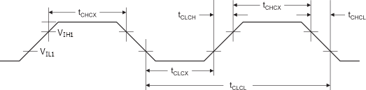
| Symbol | Description | Condition | VDD=[1.8, 5.5]V | VDD=[2.7, 5.5]V | VDD=[4.5, 5.5]V | Unit | |||
|---|---|---|---|---|---|---|---|---|---|
| Min. | Max. | Min. | Max. | Min. | Max. | ||||
| fCLCL | Frequency | 0 | 5.0 | 0.0 | 10.0 | 0.0 | 20.0 | MHz | |
| tCLCL | Clock Period | 200 | - | 100 | - | 50 | - | ns | |
| tCHCX | High Time | 80 | - | 40 | - | 20 | - | ns | |
| tCLCX | Low Time | 80 | - | 40 | - | 20 | - | ns | |
| tCLCH | Rise Time | - | 2.0 | - | 1.6 | - | 0.5 | µs | |
| tCHCL | Fall Time | - | 2.0 | - | 1.6 | - | 0.5 | µs | |
| ΔtCLCL | Change in period from one clock cycle to the next | - | 2 | - | 2 | - | 2 | % | |