The programming connector pin functions are different for various devices
and interfaces. Refer to the following pinout tables for debug and data stream
interfaces.
Note: Refer to the data
sheet for the device you are using as well as the application notes for the specific
interface for additional information and diagrams.
| MPLAB PICkit 4 | DEBUG | |||||||||||
|---|---|---|---|---|---|---|---|---|---|---|---|---|
| Connector | Pin # | Pin Name | ICSP (MCHP) | MIPS EJTAG | CORTEX® SWD | AVR® JTAG | AVR ISP(&DW) | UPDI | PDI | AW | DW(IRE) | TPI |
 |
1 | TVPP | MCLR | MCLR | MCLR | |||||||
| 2 | TVDD | VDD | VIO_REF | VTG | VTG | VTG | VTG | VTG | VTG | VTG | VTG | |
| 3 | GND | GND | GND | GND | GND | GND | GND | GND | GND | GND | GND | |
| 4 | PGD | DAT | TDO | SWO | TDO | MISO | DAT | DAT | DATA | DAT | ||
| 5 | PGC | CLK | TCK | SWCLK | TCK | SCK | CLK | |||||
| 6 | TAUX | AUX | RESET | RESET | CLK | dW | RST | |||||
| 7 | TTDI | TDI | TDI | MOSI | ||||||||
| 8 | TTMS | TMS | SWDIO | TMS | ||||||||
| MPLAB® PICkit™ 4 | DATA STREAM | |
|---|---|---|
| Pin # | DMCI / DGI U(S)ART / CDC | DGI SPI |
| 1 | ||
| 2 | VTG | |
| 3 | GND | |
| 4 | MISO | |
| 5 | SCK | |
| 6 | (SCK) | |
| 7 | TX | MOSI |
| 8 | RX | SS |
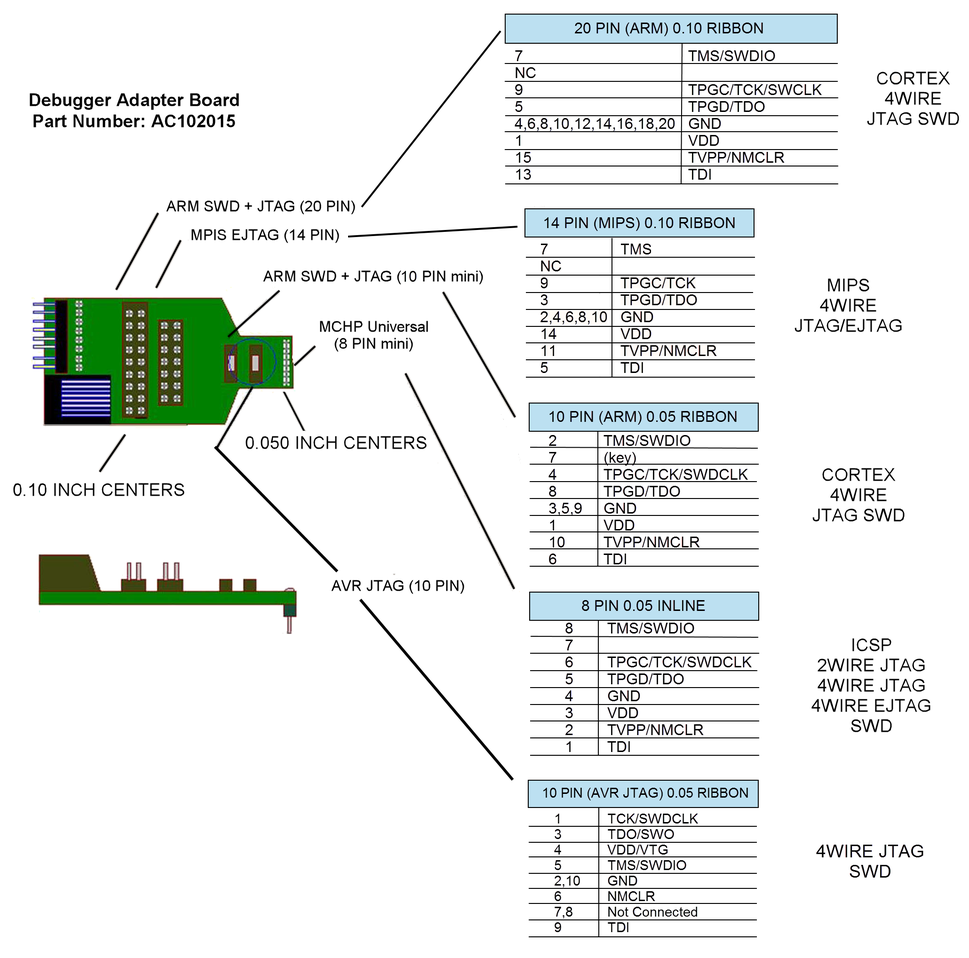
The following figure shows the debugger adapter board (AC102015) pinouts.
Figure 1. Debugger Adapter Board
Pinouts