When designing an application PCB which includes an Atmel SAM with the JTAG interface, it is recommended to use the pinout as shown in the figure below. Both 100-mil and 50-mil variants of this pinout are supported, depending on the cabling and adapters included with the particular kit.
Figure 1. SAM JTAG Header Pinout
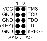
| Name | Pin | Description |
|---|---|---|
| TCK | 4 | Test Clock (clock signal from the Atmel-ICE into the target device). |
| TMS | 2 | Test Mode Select (control signal from the Atmel-ICE into the target device). |
| TDI | 8 | Test Data In (data transmitted from the Atmel-ICE into the target device). |
| TDO | 6 | Test Data Out (data transmitted from the target device into the Atmel-ICE). |
| nRESET | 10 | Reset (optional). Used to reset the target device. Connecting this pin is recommended since it allows the Atmel-ICE to hold the target device in a reset state, which can be essential to debugging in certain scenarios. |
| VTG | 1 | Target voltage reference. The Atmel-ICE samples the target voltage on this pin in order to power the level converters correctly. The Atmel-ICE draws less than 1mA from this pin in this mode. |
| GND | 3, 5, 9 | Ground. All must be connected to ensure that the Atmel-ICE and the target device share the same ground reference. |
| KEY | 7 | Connected internally to the TRST pin on the AVR connector. Recommended as not connected. |
Tip: Remember to include a
decoupling capacitor between pin 1 and GND.