| Symbol | Parameter | Min. | Max | Units |
|---|---|---|---|---|
| VPP | Programming Enable Voltage | 11.5 | 12.5 | V |
| IPP | Programming Enable Current | - | 250 | μA |
| tDVXH | Data and Control Valid before XTAL1 High | 67 | - | ns |
| tXLXH | XTAL1 Low to XTAL1 High | 200 | - | ns |
| tXHXL | XTAL1 Pulse Width High | 150 | - | ns |
| tXLDX | Data and Control Hold after XTAL1 Low | 67 | - | ns |
| tXLWL | XTAL1 Low to WR Low | 0 | - | ns |
| tXLPH | XTAL1 Low to PAGEL high | 0 | - | ns |
| tPLXH | PAGEL low to XTAL1 high | 150 | - | ns |
| tBVPH | BS1 Valid before PAGEL High | 67 | - | ns |
| tPHPL | PAGEL Pulse Width High | 150 | - | ns |
| tPLBX | BS1 Hold after PAGEL Low | 67 | - | ns |
| tWLBX | BS2/1 Hold after RDY/BSY high | 67 | - | ns |
| tPLWL | PAGEL Low to WR Low | 67 | - | ns |
| tBVWL | BS1 Valid to WR Low | 67 | - | ns |
| tWLWH | WR Pulse Width Low | 150 | - | ns |
| tWLRL | WR Low to RDY/BSY Low | 0 | 1 | μs |
| tWLRH | WR Low to RDY/BSY High(1) | 3.7 | 4.5 | ms |
| tWLRH_CE | WR Low to RDY/BSY High for Chip Erase(2) | 7.5 | 9 | ms |
| tXLOL | XTAL1 Low to OE Low | 0 | - | ns |
| tBVDV | BS1 Valid to DATA valid | 0 | 250 | ns |
| tOLDV | OE Low to DATA Valid | - | 250 | ns |
| tOHDZ | OE High to DATA Tri-stated | - | 250 | ns |
Note:
- tWLRH is valid for the Write Flash, Write EEPROM, Write Fuse bits and Write Lock bits commands.
- tWLRH_CE is valid for the Chip Erase command.
Figure 1. Parallel Programming Timing,
Including some General Timing Requirements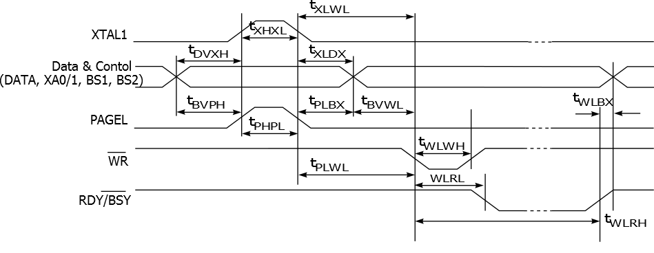
Figure 2. Parallel Programming Timing, Loading
Sequence with Timing Requirements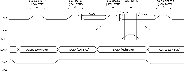
Note: The timing requirements shown in Table 1 (i.e., tDVXH, tXHXL, and tXLDX) also
apply to loading operation
Figure 3. Parallel Programming Timing, Reading
Sequence (within the Same Page) with Timing Requirements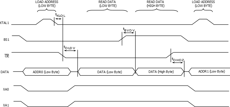
Note: The timing requirements shown in Table 1 (i.e., tDVXH, tXHXL, and tXLDX) also
apply to reading operation.