The Analog-to-Digital Converter (ADC) peripheral produces 10-bit results. The ADC input can either be internal (e.g. a voltage reference), or external through the analog input pins. The ADC is connected to an analog multiplexer, which allows selection of multiple single-ended voltage inputs. The single-ended voltage inputs refer to 0V (GND).
The ADC supports sampling in bursts where a configurable number of conversion results are accumulated into a single ADC result (Sample Accumulation). The ADC input signal is fed through a sample-and-hold circuit that ensures the input voltage to the ADC is held at a constant level during sampling.
Selectable voltage references from the internal Voltage Reference (VREF) peripheral, VDD supply voltage, or external VREF pin (VREFA).
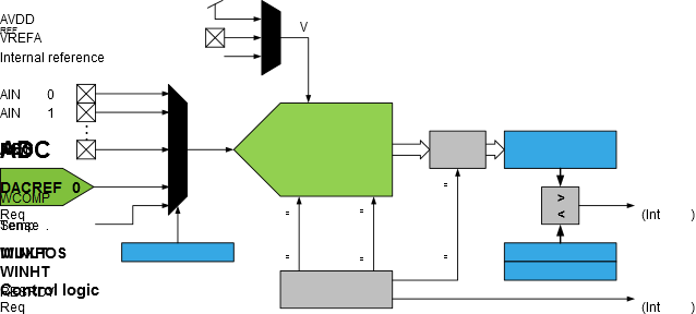
The analog input channel is selected by writing to the MUXPOS bits in the
MUXPOS register (ADCn.MUXPOS). Any of the ADC input pins, GND, internal Voltage
Reference (VREF), or temperature sensor, can be selected as single-ended
input to the ADC. The ADC is enabled by writing a ‘1’ to the ADC ENABLE
bit in the Control A register (ADCn.CTRLA). Voltage reference and input channel
selections will not go into effect before the ADC is enabled. The ADC does not consume
power when the ENABLE bit in ADCn.CTRLA is zero.