ATtiny5/10 feature an 8-bit, successive approximation ADC. The ADC is connected to a 4-channel analog multiplexer which allows four single-ended voltage inputs constructed from the pins of port B. The single-ended voltage inputs refer to 0V (GND).
The ADC contains a Sample and Hold circuit which ensures that the input voltage to the ADC is held at a constant level during conversion.
Internal reference voltage of VCC is provided on-chip.
The ADC is not available in ATtiny4/9.
The Power Reduction ADC bit in the Power Reduction Register (PRR.PRADC) must be written to '0' in order to be enable the ADC.
The ADC converts an analog input voltage to an 8-bit digital value through successive approximation. The minimum value represents GND and the maximum value represents the voltage on the voltage on VCC.
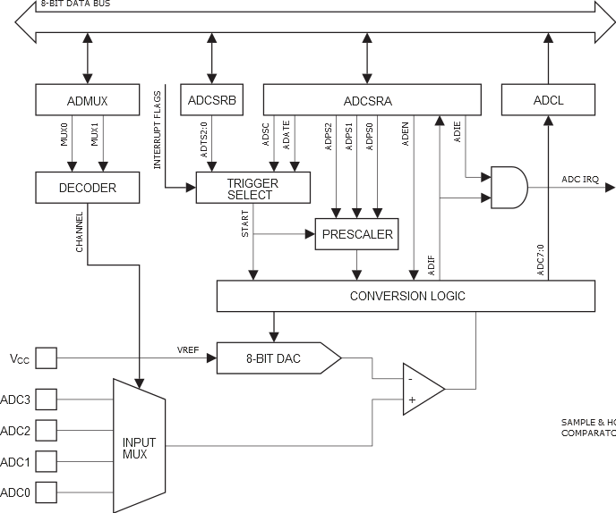
The analog input channel is selected by writing to the MUX bits in the ADC Multiplexer Selection register (ADMUX.MUX). Any of the ADC input pins can be selected as single ended inputs to the ADC. The ADC is enabled by writing a '1' to the ADC Enable bit in the ADC Control and Status Register A (ADCSRA.ADEN). Voltage reference and input channel selections will not take effect until ADEN is set. The ADC does not consume power when ADEN is cleared, so it is recommended to switch off the ADC before entering power saving sleep modes.