The following section describes the sequence of events that occur when the module is receiving data in 7-bit Addressing mode:
- 1.Depending on the configuration of the
Address Buffer Disable (ABD) bit, one of two methods may be used to
begin communication:
- 1.1.When ABD is clear (ABD =
0), the address buffer, I2CxADB1, is enabled. In this case, the 7-bit slave address and R/W bit are loaded into I2CxADB1, with the R/W bit set (R/W =1). The number of expected received data bytes are loaded into I2CxCNT. After these registers are loaded, software must set the Start (S) bit to begin communication. Once the S bit is set, master hardware waits for the Bus Free (BFRE) bit to be set before transmitting the Start condition to avoid bus collisions. - 1.2.When ABD is set (ABD =
1), the address buffer is disabled. In this case, the number of expected received data bytes are loaded into I2CxCNT, and the slave’s 7-bit address and R/W bit are loaded into I2CxTXB. A write to I2CxTXB will cause master hardware to automatically issue a Start condition once the bus is idle (BFRE =1). Software writes to the Start bit are ignored.
- 1.1.When ABD is clear (ABD =
- 2.Master hardware waits for BFRE to be set, then shifts out the Start condition. Module hardware sets the Master Mode Active (MMA) bit and the Start Condition Interrupt Flag (SCIF). If the Start Condition Interrupt Enable (SCIE) bit is set, the generic I2CxIF is also set.
- 3.Master hardware transmits the 7-bit slave address and R/W bit.
- 4.Master hardware samples SCL to determine if the slave is stretching the clock, and continues to sample SCL until the line is sampled high.
- 5.Master hardware transmits the 9th
clock pulse, and receives the ACK/NACK response from the
slave.
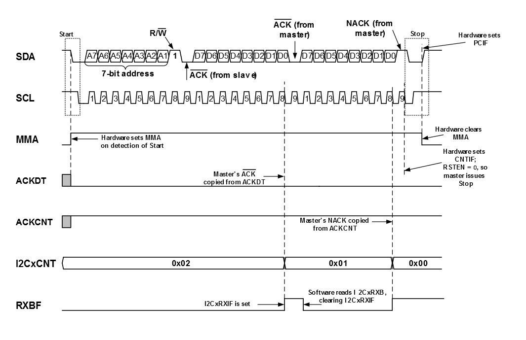
If an ACK is received, master hardware receives the first seven bits of the data byte into the receive shift register.
If a NACK is received, hardware sets the NACK Detect Interrupt Flag (NACKIF), and:- 5.1.ABD =
0: Master generates a Stop condition, or sets the MDR bit (if RSEN is also set) and waits for software to set the Start bit to generate a Restart condition. - 5.2.ABD =
1: Master generates a Stop condition, or sets the MDR bit (if RSEN is also set) and waits for software to load a new address into I2CxTXB. Software writes to the Start bit are ignored.
If the NACK Detect Interrupt Enable (NACKIE) is also set, hardware sets the generic I2CxEIF bit.
- 5.1.ABD =
- 6.If previous data remains in the
I2C Receive Buffer (I2CxRXB) when the first seven bits of the new byte are received into the
receive shift register (RXBF =
1), the MDR bit is set (MDR =1), and the clock is stretched after the 7th falling edge of SCL. This allows the master time to read I2CxRXB, which clears the RXBF bit, and prevents receive buffer overflows. Once RXBF is clear, hardware releases SCL. - 7.The master clocks in the 8th bit of the data byte into the receive shift register, then transfers the full byte into I2CxRXB. Master hardware sets the I2C Receive Interrupt Flag (I2CxRXIF) and RXBF, and if the I2C Receive Interrupt Enable (I2CxRXIE) is set, the generic I2CxIF is also set. Finally, I2CxCNT is decremented by one.
- 8.Master hardware checks I2CxCNT for a
zero value.If I2CxCNT is non-zero (I2CxCNT !=
0), hardware transmits the value of the Acknowledge Data (ACKDT) bit as the acknowledgement response to the slave. It is up to user software to properly configure ACKDT. In most cases, ACKDT should be clear (ACKDT =0), which indicates an ACK response.If I2CxCNT is zero (I2CxCNT =0), hardware transmits the value of the Acknowledge End of Count (ACKCNT) bit as the acknowledgement response to the slave. CNTIF is set, and master hardware either issues a Stop condition or a Restart condition. It is up to user software to properly configure ACKCNT. In most cases, ACKCNT should be set (ACKCNT =1), which indicates a NACK response. When hardware detects a NACK on the bus, it automatically issues a Stop condition. If a NACK is not detected, the Stop will not be generated, which may lead to a stalled bus condition. - 9.Master hardware receives the first seven bits of the next data byte into the receive shift register.
- 10.Repeat Steps 6 – 9 until all expected bytes have been received.
Figure 1. 7-Bit Master Mode
Reception