The following section describes the sequence of events that occur when the module is receiving data in 7-bit Addressing mode:
- 1.The master issues a Start condition. Once the Start is detected, slave hardware sets the Start Condition Interrupt Flag (SCIF) bit. If the Start Condition Interrupt Enable (SCIE) bit is also set, the generic I2CxIF bit is also set.
- 2.The master transmits the 7-bit slave address with the R/W bit clear, indicating that it intends to write data to the slave.
- 3.The received address is compared to
the values in the I2CxADR registers. If the slave is configured in 7-bit Addressing
mode (no masking), the received address is independently compared to each of the
I2CxADR0/1/2/3 registers. In 7-bit Addressing with Masking mode, the received
address is compared to the masked value of I2CxADR0 and I2CxADR2.
If an address match occurs:
- The Slave Mode Active (SMA) bit is set by module hardware.
- The R/W bit value is copied to the Read Information (R) bit by module hardware.
- The Data (D) bit is cleared (D =
0) by hardware, indicating the last received byte was an address. - The Address Interrupt Flag
(ADRIF) bit is set (ADRIF =
1). If the Address Interrupt and Hold Enable (ADRIE) bit is set (ADRIE =1), and the Clock Stretching Disable (CSD) bit is clear (CSD =0), hardware sets the Slave Clock Stretching (CSTR) bit and the generic I2CxIF bit. This allows time for the slave to read either I2CxADB0 or I2CxRXB and selectively ACK/NACK based on the received address. When the slave has finished processing the address, software must clear CSTR to resume operation. - The matching received address
is loaded into either the I2CxADB0 register or into the I2CxRXB register as
determined by the Address Buffer Disable (ABD) bit. When ABD is clear (ABD =
0), the matching address is copied to I2CxADB0. When ABD is set (ABD =1), the matching address is copied to I2CxRXB, which also sets the Receive Buffer Full Status (RXBF) bit and the I2C Receive Interrupt Flag (I2CxRXIF) bit. I2CxRXIF is a read-only bit, and must be cleared by either reading I2CxRXB or by setting the Clear Buffer (CLRBF) bit (CLRBF =1).
If no address match occurs, the module remains idle.
- 4.The master device transmits the 9th
clock pulse, and slave hardware transfers the value of the ACKDT bit onto the SDA line. If there are
pending errors, such as a receive overflow (RXO =
1), slave hardware automatically generates a NACK condition. NACKIF is set, and the module goes idle. - 5.Upon the 9th falling SCL edge, the
Acknowledge Status Time Interrupt Flag (ACKTIF) bit is set. If the Acknowledge
Interrupt and Hold Enable (ACKTIE) bit is also set, the generic I2CxIF is
set, and if slave hardware generated an ACK, the CSTR bit is also set and the clock is stretched
(when CSD =
0). If a NACK was generated, the CSTR bit remains unchanged. Once complete, software must clear CSTR and ACKTIF to release the clock and continue operation. - 6.If slave hardware generated a NACK, master hardware generates a Stop condition, the Stop Condition Interrupt Flag (PCIF) bit is set when slave hardware detects the Stop condition, and the slave goes idle. If an ACK was generated, master hardware transmits the first seven bits of the 8-bit data byte.
- 7.If data remains in I2CxRXB (RXBF =
1and I2CxRXIF =1) when the first seven bits of the new byte are received by the shift register, CSTR is set, and if CSD is clear, the clock is stretched after the 7th falling edge of SCL. This allows time for the slave to read I2CxRXB, which clears RXBF and I2CxRXIF, and prevents a receive buffer overflow. Once RXBF and I2CxRXIF are cleared, hardware releases SCL. - 8.Master hardware transmits the 8th bit
of the current data byte into the slave receive shift register. Slave hardware then
transfers the complete byte into I2CxRXB on the 8th falling edge of SCL, and sets the following bits:
I2CxCNT is decremented by one. If the Data Write Interrupt and Hold Enable (WRIE) is set (WRIE =
1), hardware sets CSTR (when CSD =0) and stretches the clock, allowing time for slave software to read I2CxRXB and determine the state of the ACKDT bit that is transmitted back to the master. Once the slave determines the acknowledgement response, software clears CSTR to allow further communication. - 9.Master hardware transmits the 9th
clock pulse. If there are pending errors, such as receive buffer overflow, slave
hardware automatically generates a NACK condition, sets NACKIF, and the module goes idle. If I2CxCNT is non-zero (I2CxCNT !=
0), slave hardware transmits the value of ACKDT as the acknowledgement response to the master. It is up to software to configure ACKDT appropriately. In most cases, the ACKDT bit should be clear (ACKDT =0) so that the master receives an ACK response (logic low level on SDA during the 9th clock pulse).If I2CxCNT is zero (I2CxCNT =0), slave hardware transmits the value of the Acknowledge End of Count (ACKCNT) bit as the Acknowledgement response, rather than the value of ACKDT. It is up to software to configure ACKCNT appropriately. In most cases, ACKCNT should be set (ACKCNT =1), which represents a NACK condition. When master hardware detects a NACK on the bus, it will generate a Stop condition. If ACKCNT is clear (ACKCNT =0), an ACK will be issued, and master hardware will not issue a Stop condition. - 10.Upon the 9th falling edge of SCL, the ACKTIF bit is set. If ACKTIE is also set, the generic I2CxIF is set, and if CSD is clear, slave hardware sets CSTR and stretches the clock. This allows time for software to read I2CxRXB. Once complete, software must clear both CSTR and ACKTIF to release the clock and continue communication.
- 11. Repeat steps 6 -10 until the master
has transmitted all the data (I2CxCNT =
0), or until the master issues a Stop or Restart condition.
Figure 1. 7-Bit Slave Mode Reception (No
Clock Stretching)
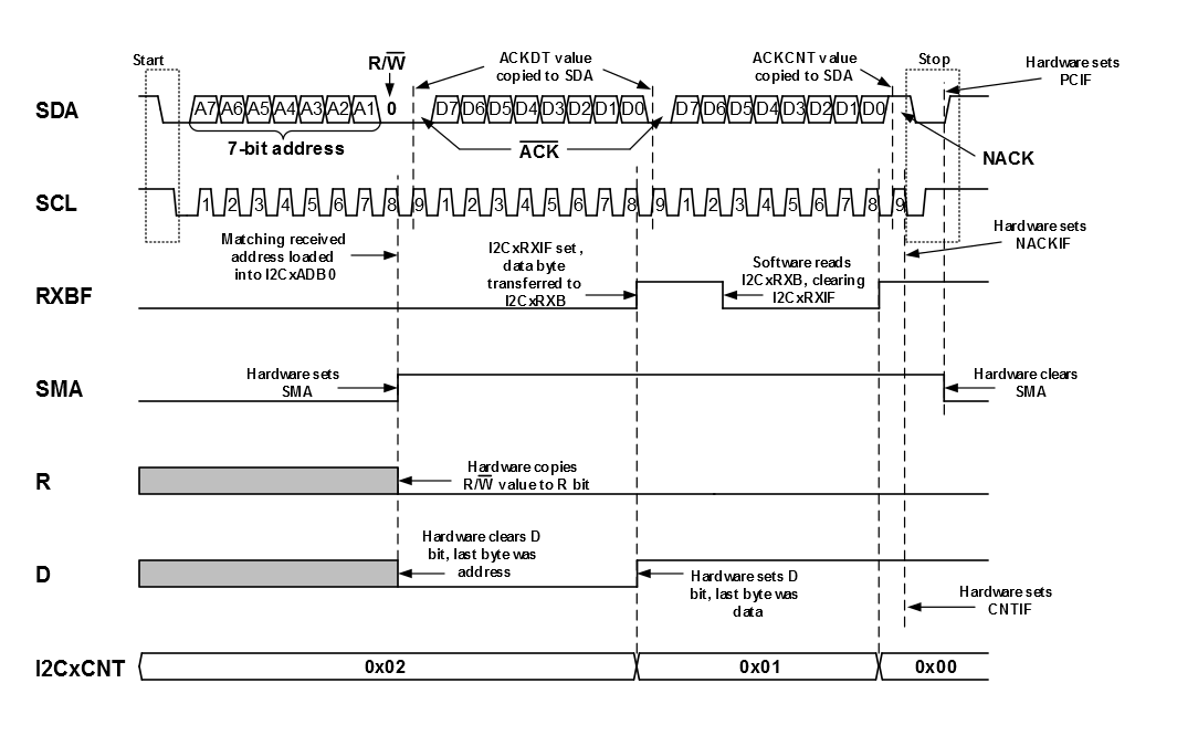
Figure 2. 7-Bit Slave Mode Reception (ADRIE
= 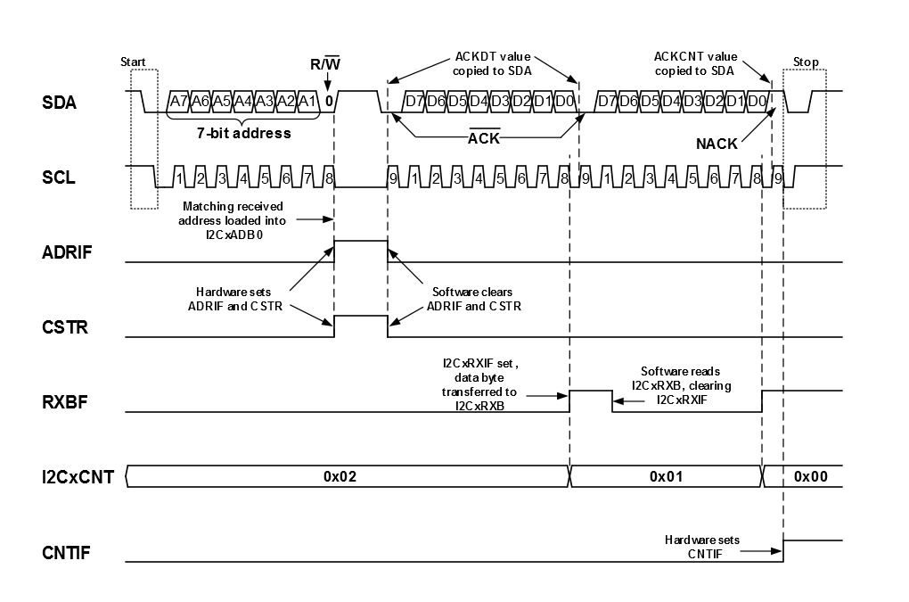
1)
Figure 3. 7-Bit Slave Mode Reception (ACKTIE
= 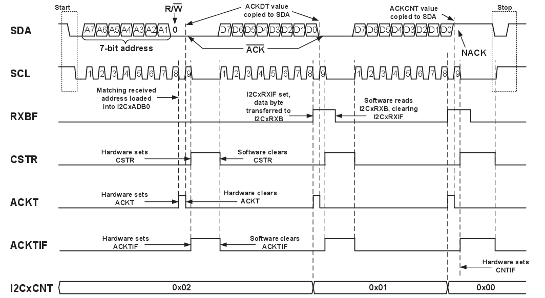
1)
Figure 4. 7-Bit Slave Mode Reception (WRIE =
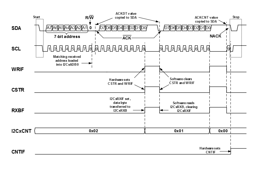
1)